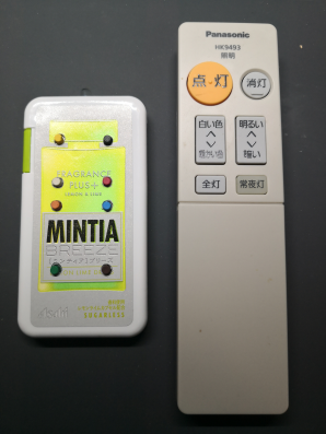
I Made a Button Battery-Powered Ceiling Light Remote Control Using ATtiny13A [PCB & Case Fabrication Edition]
Back to TopTo reach a broader audience, this article has been translated from Japanese.
You can find the original version here.
The previous article is here 【Development Edition】
Case Selection
#In the Development Edition, I built the remote control on a breadboard.
However, its size is too big and the wiring is exposed, so it cannot be operated by hand and does not serve well as a remote control replacement. Therefore, I decided to assemble the circuit on a PCB and enclose it in a case for everyday use.
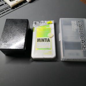
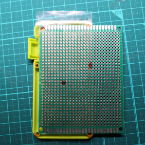
For now, I prepared a few items that might serve as a case.
- Left: Small generic plastic case
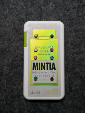
- Center: Mintia Breeze Lemon Lime Dress
- Right: Semi-transparent card case
While enjoying a day off shopping with my wife, I purchased the plastic case at the usual Akizuki and, as a backup, chose the card case from a 100-yen shop. Both have sufficient height (thickness) to accommodate the PCB, but I felt they were too large to serve as a remote control. On the way home, I stopped by a supermarket for groceries, and while my wife was in line at the register, I noticed Mintia right beside her. I thought, “This is it,” and quietly slipped it into our shopping basket. I ended up getting hooked on picking it up as an extra.
Mintia fits perfectly in the hand, and its thickness is about the same as that of the remote control. I started to fantasize that if I could realize this size, it would make for a great article.
PCB Processing
#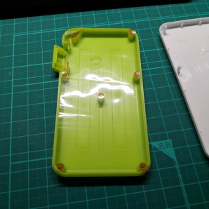
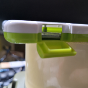
I immediately transferred the tablet (contents) and opened the case. It turned out that the case has a surprisingly good height and is robust. With a central support, the case does not collapse. However, I anticipated that the limited layout would make assembling the circuit challenging.
Aligning the PCB with the case.
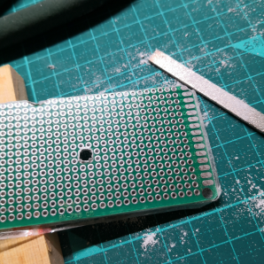
I applied transparent tape to the PCB, cut it with a rotary tool to match the case size, and drilled holes with an electric drill. I then fine-tuned the dimensions with a file.
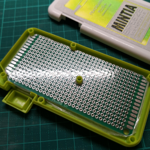
When the PCB was inserted into the case, it fit perfectly. I secured the PCB using the outlines of each support, without resorting to screws. The positions of the supports on the left and right were slightly different, so I had some difficulty with fine adjustments.
Looking at the PCB inside the case from the tablet extraction opening, there is extra space at the top. In practice, because wiring will also be routed on the back side, the PCB will be positioned a bit higher. Even so, it occupies less than half the available space, leaving room on the PCB for the ATtiny13A microcontroller and the encoder. I even began to feel that Mintia might have been made just for this purpose.
I roughly determined the positions of the buttons. Since I planned to match the layout of the existing remote control’s buttons, I arranged them accordingly. Also, considering Mintia’s package design, I searched for positions that would minimize covering any text. I chose button colors that best suited their respective functions.
PCB Design
#Now, let’s move on to PCB design.
I designed the PCB using BSch3V, a simple and easy-to-use CAD program for circuit diagrams. Since it allows drawings to be described in layers, I made full use of this feature.
Please consider the design data as a casual doodle. I have never done PCB design professionally and used the CAD software by mimicking what I saw. Note that my use of design elements (such as bus lines and junction points) is quite unconventional.
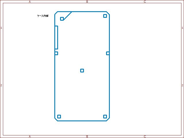
On Layer 1, I drew the "inside of the case". Since the alignment between the PCB dimensions and the case was already set, I sketched the internal structure of the case and the positions of the supports to match the PCB. Generally, the pitch between PCB lands is 2.54mm (0.1 inch), and since the CAD program allows lines to be drawn to this specification, the dimensions match perfectly.
The copper foil areas on a PCB where components are soldered are called “lands.”
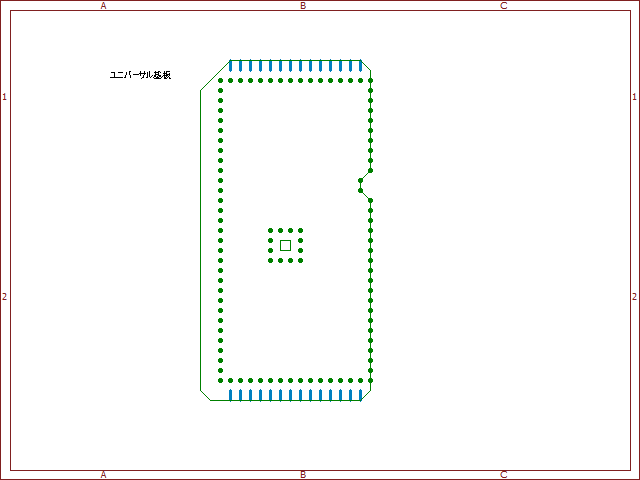
On Layer 2, I drew the "universal PCB". I only plotted the lands (represented as dots) around the outer edge and the holes for the central support. Components will be mounted within these land areas.
I’ve been referring to it simply as a “PCB,” but a board that allows free placement of components and wiring is technically called a “universal PCB.” In contrast, a board where the placement of components and wiring is predetermined is known as a “printed circuit board.”
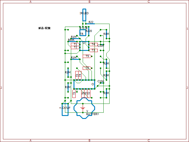
On Layer 3, I drew the "components & wiring". While the positions of the buttons and the infrared LED are nearly set, the key challenge was how to lay out the other components.
- Where should the microcontroller and encoder be placed?
- How can I simplify the wiring?
- How can I prevent wiring from crossing?
- How should the wiring be allocated between the front and back sides?
I revised the layout several times and finally settled on this design. It was a real challenge, but by separating the layers, making adjustments was relatively easy. I definitely couldn’t have done this without using CAD.
Regarding the diagram’s labels Tn (n = 1 to 6): For example, T1 indicates that one T1 is connected to another T1. Since it was impossible to avoid crossing wires, T1 through T6 are connected using vinyl wires as free-hanging wiring.
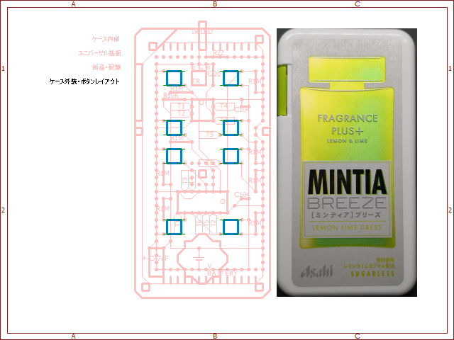
On Layer 4, I drew the "case exterior & button layout". All layers are displayed. By overlaying the imported Mintia case image onto the design, I could verify the positions of the buttons.
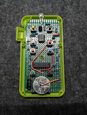
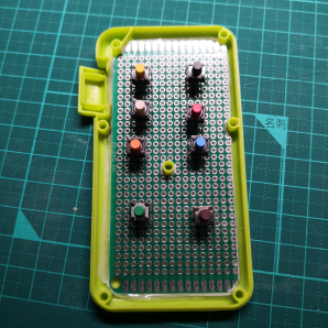
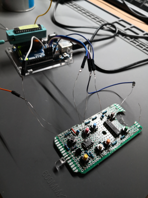
Based on the CAD design, I soldered the components onto the PCB and installed it in the case.
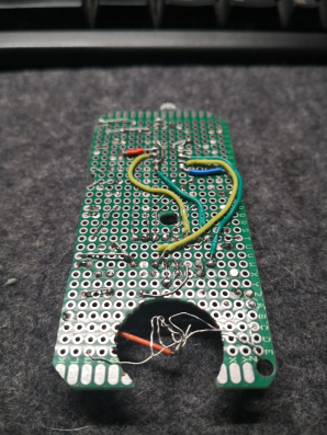
This is a view of the PCB from the back, and you can see wires floating in various places. This is because the copper foil on the lands connects both sides; if a wire touches the land, it can contact a wire on the front side. I had not taken this into account.
Since the button battery would not fit into the Mintia case if housed in a battery holder, I cut out a section of the PCB corresponding to the diameter of the button battery and fitted it there.
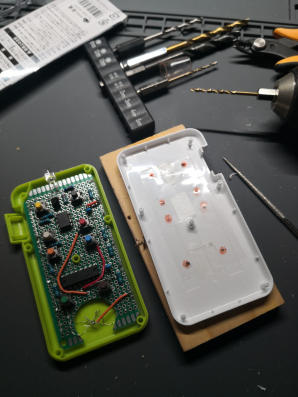
Finally, I drilled holes for the buttons in the Mintia case, and it was finished.
...Or so I thought, but I had forgotten to program the ATtiny13A! Gah 😢
I had overlooked that I had mounted a second ATtiny13A separate from the breadboard version. Removing the ATtiny13A now wouldn’t be easy. In a last-minute rush, I extended wires from an Arduino (programmer) and soldered them to the ATtiny13A to program it.
Burn!! It’s complete. The soldering was flawless, and it worked on the first try. I was convinced that something must be wrong somewhere, but I’m quite pleased with the result.
By the way, I think the most expensive component was Mintia, which cost around 200 yen. The total parts cost was under 1000 yen.
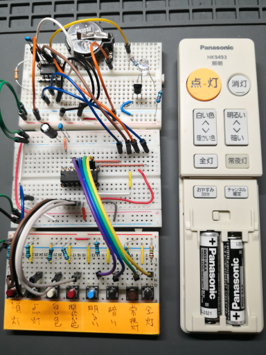
Now, please take a look at the finished product. (It emits a "pi" sound, so please be careful!!)
I pressed the buttons in the following order:
- Light On
- White (long press)
- Warm (long press)
- Brighter (long press)
- Dimmer (long press)
- All On
- Night Light
- Light Off
Conclusion
#An indispensable resource in creating this infrared remote control was the datasheet for the ATtiny13A (AVR microcontroller). Until now, I had only written programs using the Arduino API and had never directly read an AVR microcontroller datasheet. By reading the datasheet, I was able to shed light on aspects of the microcontroller that I had never consciously considered, deepening my understanding of both Arduino and AVR microcontrollers.